



Introduction
A transistor is a semiconductor device that can control electrical current. A transistor symbol is the simple graphic used to show this device in a circuit diagram. This article explains common transistor symbols, their structures, operating modes, and how to identify them.
What Is a Transistor?
A transistor is a semiconductor device with three or more terminals. It can control current or voltage in a circuit. Transistors are widely used for switching and signal amplification.
How Does a Transistor Work?
A transistor uses a small electrical signal to control a larger current or voltage. The exact control method depends on the transistor type. For example, a BJT uses the base to control current between the collector and emitter, while a FET uses the gate voltage to control current between the drain and source.
For a BJT, the amount of base drive affects the collector current. This allows the transistor to work in different regions. The three common BJT regions are cutoff, active, and saturation.
- Cut-off: The transistor is essentially off, so collector current is very small.
- Active: The transistor controls collector current and can be used for amplification.
- Saturation: The transistor is strongly on and allows the load current to reach the circuit limit.
|
Region |
State |
Function |
Examples of Use |
|
Cut-off |
OFF |
Blocks collector current |
Electronic switch OFF |
|
Active |
Controlled |
Controls collector current |
Signal amplifier |
|
Saturation |
ON |
Allows high collector current |
Electronic switch ON |
What Does a Transistor Do?
A transistor has several important functions:
- As a switch: It can turn current on or off. This is common in digital circuits and control circuits.
- As an amplifier: It can use a smaller input signal to control a larger output signal. This makes it useful in audio and other signal circuits.
- As a current-control device: It can regulate the current flowing through part of a circuit.
What Is a Transistor Symbol?
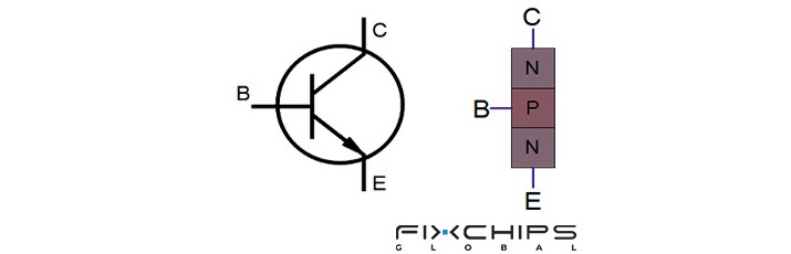
A transistor symbol is a graphical representation of a transistor in a schematic. It shows the transistor type and its terminals without drawing the physical device.
The symbol helps the reader understand how the transistor is connected and how it should function in the circuit. IEC 60617 is an international source for graphical symbols used in electrotechnical diagrams, including semiconductor devices.
Why Use Symbols for Transistors?
Standard symbols make circuit diagrams easier to read:
- Show the device type: The symbol helps identify a BJT, JFET, MOSFET, or other transistor.
- Show the terminals: Letters and connection lines identify terminals such as B, C, E, G, D, and S.
- Show key features: Arrows, gates, channels, and other marks can indicate important device characteristics.
- Make diagrams easier to understand: Engineers can read the circuit without seeing the physical transistor.
- Support standard documentation: Standardized graphical symbols make circuit diagrams easier to share and interpret.
Bipolar Junction Transistor (BJT) Symbol
A Bipolar Junction Transistor (BJT) is a three-terminal transistor in which a small base current controls a larger collector current. The two basic types are NPN and PNP. A special BJT arrangement is the Darlington Pair.
Symbol Analysis
The three terminals of a BJT are:
B — Base: The control terminal.
C — Collector: The terminal through which collector current flows.
E — Emitter: The terminal through which emitter current flows.
The BJT symbol has three connection lines:
The base is connected to the center region. The other two connections are the collector and emitter. An arrow is placed on the emitter side. The arrow shows the direction of conventional current at the emitter-base junction.
How Does a BJT Work?
- NPN: A small base current allows a larger conventional current to flow from the collector toward the emitter. In the normal active region, the base-emitter junction is forward biased and the base-collector junction is reverse biased.
- PNP: The current and voltage polarities are reversed compared with an NPN transistor. Conventional current flows into the emitter and out toward the collector when the PNP device is operating normally.
Identifying NPN vs. PNP
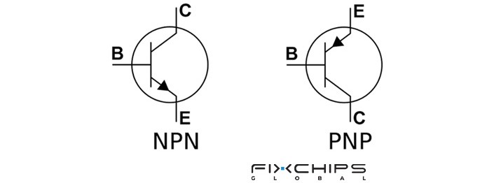
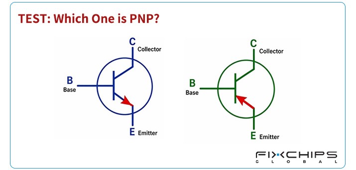
The symbols look similar, but the emitter arrow points in different directions.
- NPN: The emitter arrow points out.
- PNP: The emitter arrow points in.
- Easy memory rule:
NPN = Not Pointing iN.
PNP = Pointing iN.
The arrow refers to conventional current direction, not electron movement. This distinction is important when reading transistor symbols.
Special BJT: Darlington Pair
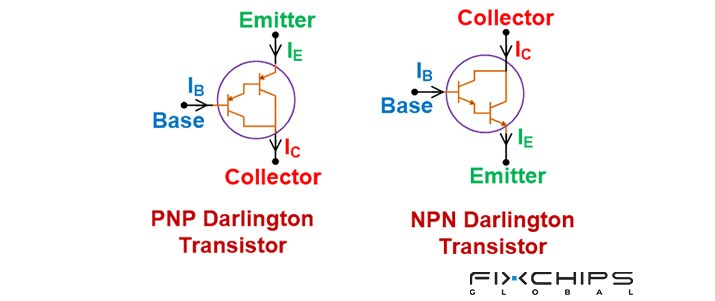
A Darlington Pair uses two bipolar transistors connected together so that their current gains combine. This arrangement provides a much higher overall current gain than a single transistor.
Its symbol looks like two BJT symbols combined into one device. The two transistors are internally connected, while the external circuit normally sees the combined base, collector, and emitter connections.
Field-Effect Transistor (FET) Symbol
A Field-Effect Transistor (FET) controls current by using an electric field. Its main terminals are the gate, drain, and source. Common FET families include the JFET and MOSFET.
The three main FET terminal letters are:
D — Drain: The terminal associated with the drain side of the channel.
S — Source: The terminal associated with the source side of the channel.
G — Gate: The control terminal.
Type 1: Junction Field-Effect Transistor (JFET) Symbol
A Junction Field-Effect Transistor (JFET) controls the current in a semiconductor channel by changing the voltage applied to its gate. The two basic types are N-channel JFET and P-channel JFET.
JFET Symbol Analysis
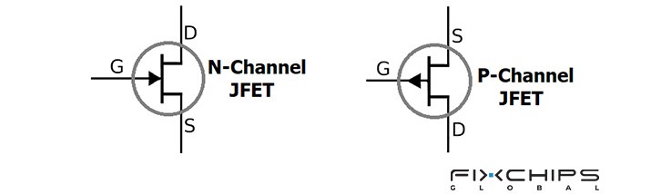
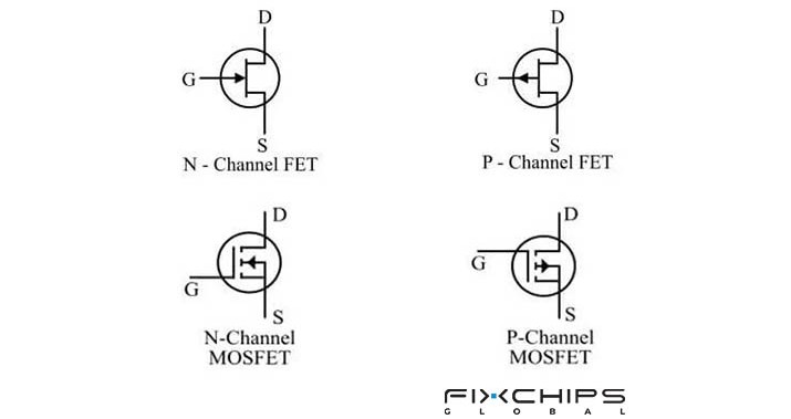
The JFET symbol has a channel between the Drain (D) and Source (S). The Gate (G) is drawn next to the channel.
The arrow on the gate shows the direction of conventional current at the gate-channel junction. In common JFET symbols, the N-channel and P-channel versions use opposite arrow directions.
How Does a JFET Work?
- N-channel JFET: The gate voltage is normally negative relative to the source. Increasing the reverse bias widens the depletion region and reduces the available channel current.
- P-channel JFET: The basic operation is similar, but the voltage polarities and current directions are reversed compared with an N-channel JFET.
In both types, the gate voltage controls the channel between the drain and source.
Identifying N-Channel vs. P-Channel JFET
- N-channel: Gate arrow points in toward the channel in the common schematic convention.
- P-channel: Gate arrow points out from the channel.
- Memory tip:
N-channel = arrow in.
P-channel = arrow out.
The arrow rule is different from the BJT memory rule, so it is important to identify the transistor family first.
Type 2: Metal-Oxide-Semiconductor Field-Effect Transistor (MOSFET) Symbol
A Metal-Oxide-Semiconductor Field-Effect Transistor (MOSFET) uses an insulated gate to control the current path between the drain and source. MOSFETs are widely used in switching and power-control circuits.
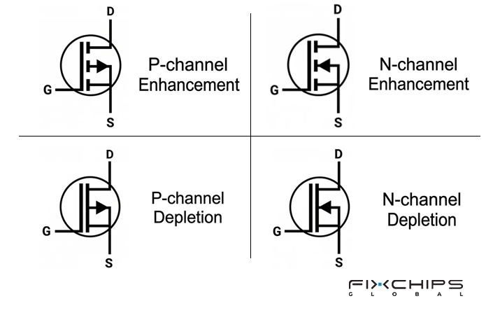
MOSFET symbols can be classified by two main features: enhancement or depletion mode, and N-channel or P-channel.
MOSFET Operating Modes
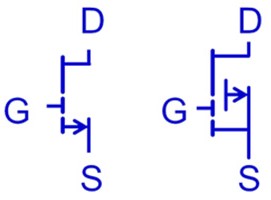
- Enhancement-mode: The channel is normally absent when the required gate-to-source voltage is not applied. Applying the proper gate voltage creates the conducting channel. In simple terms, it is normally off . This is indicated in the symbols by a intermittent line.
- Depletion-mode: A conducting channel exists when the gate-to-source voltage is zero. The proper gate voltage reduces the channel current. In simple terms, it is normally on. This is indicated in the symbols by a continuous line.
- N-channel vs. P-channel: These indicate the type of channel used by the MOSFET. Their operating voltage polarities and current directions are opposite. Both enhancement-mode and depletion-mode can be made with N-channel or P-channel structures.
Insulated-Gate Bipolar Transistor (IGBT) Symbol
An Insulated-Gate Bipolar Transistor (IGBT) combines an insulated-gate input structure with bipolar transistor behavior. It is mainly used for switching and controlling relatively high voltage and current in power electronics.
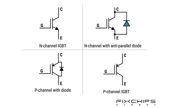
The IGBT symbol has three main terminals:
G — Gate
C — Collector
E — Emitter
The gate receives the control signal, while the collector and emitter form the main current path.
Special Transistors
Besides common BJT, JFET, MOSFET, and IGBT devices, circuit diagrams can contain other transistor types.
|
Transistor Type | Images |
|
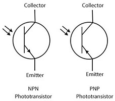
Phototransistor Symbol |
|
|
Gan Transistor Symbol |
|
|
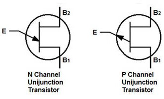
UJT Symbol |
|
|
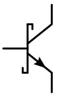
Schottky Transistor Symbol |
|
How to Identify a Transistor Symbol
Identifying a transistor symbol is easier when you check its terminals, arrows, and internal structure step by step.
Step 1: Check the terminal labels
Start by looking at the letters beside the terminals.
- B, C, E: BJT
- G, D, S: FET
- G, C, E: IGBT
Step 2: Look for an arrow
Check whether the symbol has an arrow and where it is placed.
- BJT: Arrow on the emitter
- JFET: Arrow on the gate
- NPN: Arrow points out
- PNP: Arrow points in
Step 3: Check the gate structure
Look at how the gate is connected to the channel.
- JFET: Gate forms a junction with the channel
- MOSFET: Gate is insulated from the channel
Step 4: Check the channel line
For a MOSFET, check the channel shown between the drain and source.
- Enhancement-mode: Dashed/broken line, normally off
- Depletion-mode: Solid line, normally on
Step 5: Look for special structures
Some transistor symbols contain extra structures that identify their type.
- Darlington Pair: Two BJT structures combined
- Phototransistor: Light-sensitive symbol
- IGBT: Gate with collector and emitter terminals
Common Mistakes When Identifying Transistor Symbols
Mistake 1: Confusing NPN and PNP
Problem: Both BJT symbols have the same three-terminal structure, and the main visible difference is only the direction of the emitter arrow.
Solution: Check the emitter arrow. NPN points out; PNP points in.
Mistake 2: Confusing BJT and FET
Problem: Both symbols can include an arrow, but the arrow is placed on the emitter in a BJT and on the gate in a JFET.
Solution: Check the terminal letters. B-C-E indicates a BJT, while G-D-S indicates a FET.
Mistake 3: Confusing enhancement and depletion MOSFETs
Problem: Their symbols are very similar, with the main difference shown by whether the channel line is continuous or broken.
Solution: Check the channel representation and the device label. Enhancement MOSFETs use dashed/broken line, while depletion MOSFETs use solid line.
Mistake 4: Relying only on the symbol
Problem: A symbol does not show every electrical rating or specification.
Solution: Check the part number and datasheet when exact voltage, current, or operating limits are required.
Frequently Asked Questions
What does a transistor symbol look like?
A transistor is represented by a schematic symbol that shows its type and terminals. For example, a BJT symbol has three terminals: base, collector, and emitter, while FET symbols use gate, drain, and source.
What does the arrow on a transistor symbol indicate?
For a BJT, the arrow is placed on the emitter and shows the direction of conventional current flow at the emitter. It also helps distinguish NPN and PNP transistors: the NPN arrow points outward, while the PNP arrow points inward.
Why are transistor symbols important in circuit diagrams?
Transistor symbols provide a simple way to show the transistor type, terminals, and key features in a schematic. They allow readers to understand how the device is connected without needing to draw the physical component.
What are the main applications of transistors?
Transistors are commonly used as switches and amplifiers in electronic circuits. Depending on the device and circuit design, they can also be used for functions such as signal control, filtering, rectification, and oscillation.
What are the three terminals of a transistor called?
For a BJT, the three terminals are called the base, collector, and emitter. For a FET, they are called the gate, drain, and source, so the terminal names depend on the transistor type.


