



The NE555N Timer is a general-purpose timing IC used to create time delays, pulses, and repeated signals. This article explains its function, internal structure, pins, operating modes, manufacturers, alternatives, advantages, disadvantages, and common applications.
Overview of the NE555N Timer
The NE555N is a bipolar 555 timer that uses external resistors and capacitors to control timing. It can work as a timer or oscillator and is commonly used for pulse generation, time delays, and other timing circuits. It is widely used in simple electronic circuits because of its simple design, 8-pin package, and ability to source or sink relatively high output current.
Function of the NE555N Timer
The NE555N can perform several timing functions in a circuit:
- Time delay: It can keep the output in a selected state for a set period determined by external R-C components.
- Pulse generation: It can produce a single output pulse after receiving a trigger signal.
- Oscillation: In astable mode, it continuously switches between high and low output states.
- Frequency generation: External resistors and a capacitor can set the output frequency.
- Pulse-width control: The timing network can be used to control the duration of an output pulse.
- Missing-pulse detection: A 555 monostable circuit can detect when expected pulses stop or become too far apart.
Specifications of the NE555N Timer
| Attribute | Value |
|
Supply voltage |
4.5 V to 16 V |
|
Supply current |
About 2 mA typical under the specified product conditions |
|
Maximum output current |
Up to ±200 mA |
|
Operating temperature |
0°C to 70°C for the commercial NE555 |
|
Maximum recommended frequency |
Up to 100 kHz for typical astable operation |
|
Package type |
8-pin DIP/N package |
The NE555N Timer's History
The 555 timer was designed by Hans Camenzind while he was working with Signetics in 1971.
The original 555 design was developed as a simple timing circuit that could also work as an oscillator. The design later became a widely used family of 555 timer devices and was produced in different versions and technologies.
Inner Structure of the NE555N Timer
The NE555N can be easier to understand when its internal circuit is divided into several simple blocks. Each block has a specific job in controlling the output timing.
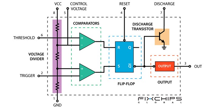
Voltage Divider
The internal voltage divider creates reference levels for the comparators. These levels are approximately one-third and two-thirds of the supply voltage, giving the timer clear points at which its state changes.
Comparators
The two comparators check the external voltage against the internal reference levels. One monitors the trigger level, while the other monitors the threshold level, and their results control the internal flip-flop.
SR Flip-Flop
The SR flip-flop stores the current state of the timer. A trigger signal can set it and make the output high, while the threshold circuit or reset input can reset it and make the output low.
Discharge Transistor
The discharge transistor provides a path for the timing capacitor to discharge. When the output is low, the discharge pin provides a low-impedance path toward ground.
Output Stage
The output stage converts the internal logic state into the external output signal. The NE555 output can source or sink up to 200 mA under the specified conditions, allowing it to drive many small loads directly.
Pin Configuration of the NE555N Timer
The NE555N uses an 8-pin configuration. Each pin connects the external circuit to a specific part of the timer's internal timing system.
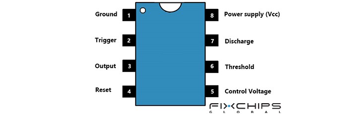
|
Pin |
Name |
Function |
|
1 |
GND |
Connects the timer to ground and provides the reference point for the circuit. |
|
2 |
TRIGGER |
Starts a timing cycle when its voltage falls below approximately 1/3 of VCC. |
|
3 |
OUTPUT |
Provides the timer's output signal and can source or sink up to 200 mA under specified conditions. |
|
4 |
RESET |
An active-low control input that can reset the internal flip-flop and force the output low. |
|
5 |
CONTROL VOLTAGE |
Provides access to the internal reference level and can be used to change the normal comparator thresholds. |
|
6 |
THRESHOLD |
Monitors the timing capacitor voltage and resets the internal flip-flop when the voltage rises above the threshold level. |
|
7 |
DISCHARGE |
Connects the timing capacitor to the discharge path when the timer is in the appropriate state. |
|
8 |
VCC |
Supplies power to the timer; the NE555 is specified for operation from 5 V to 15 V in the current TI product description, with the current device absolute operating range extending to 16 V. |
How Does the NE555N Timer Work?
The NE555N timer mainly works by watching the voltage on an external timing capacitor. Its voltage-divider network creates reference levels, the comparators check the capacitor and trigger voltages, and the SR flip-flop changes the output state according to those results.
For example, in a monostable circuit, a trigger pulse makes the output go high. The capacitor then charges through a resistor. When its voltage reaches about two-thirds of VCC, the threshold comparator resets the flip-flop, the output goes low, and the discharge transistor provides a path for the capacitor to discharge.
Operating Modes of the NE555N Timer
The NE555N can be connected in different ways to perform different timing functions. The three common modes are monostable, astable, and bistable operation.
Monostable Mode
In monostable mode, the voltage divider provides reference levels for the two comparators. When the Trigger voltage falls below about one-third of VCC, the trigger comparator sets the SR flip-flop, making the Output high and turning off the Discharge Transistor.
The external capacitor then charges through the resistor until its voltage reaches about two-thirds of VCC. The threshold comparator then resets the flip-flop, making the Output low and turning on the Discharge Transistor to discharge the capacitor.
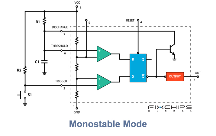
For external connections, a resistor and a capacitor are connected to the timing section, while the Trigger pin receives an external pulse. The timing components determine how long the output remains high, so this mode is commonly used for time delays and single-pulse generation.
Astable Mode
In astable mode, the timing capacitor continuously charges and discharges between about one-third and two-thirds of VCC.
The comparators detect these voltage levels and control the SR flip-flop, while the Discharge Transistor provides the discharge path; as a result, the Output continuously switches between high and low states.
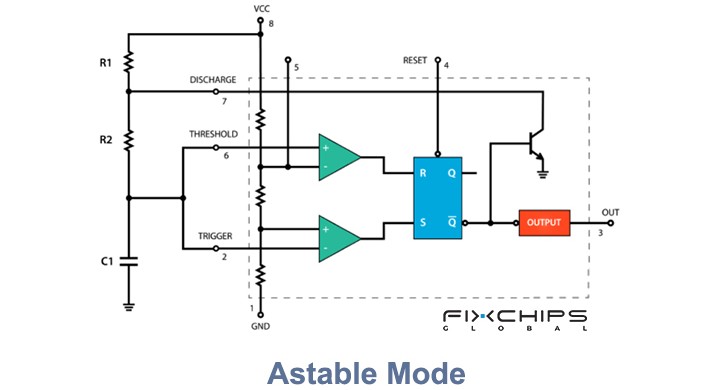
For external connections, resistors and a capacitor are connected between VCC, the Discharge pin, the Threshold/Trigger node, and ground. The resistor and capacitor values set the charging and discharging times, so this mode is mainly used for continuous pulse generation and oscillator circuits.
Bistable Mode
In bistable mode, the SR flip-flop stores one of two output states.
The Trigger comparator can set the flip-flop and make the Output high, while the Reset input can clear the flip-flop and make the Output low; the internal discharge path is not used as the main timing element because there is no timing capacitor controlling the state.
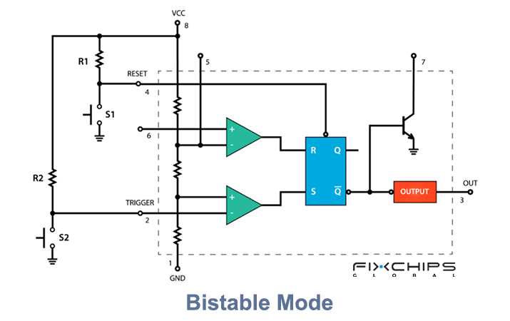
For external connections, the Trigger and Reset pins are used as control inputs, while the Output provides the selected high or low state. Because the output remains in its current state until a control signal changes it, this mode can be used for simple switching and state-control circuits.
NE555N Operating Modes Comparison
|
Comparison |
Monostable |
Astable |
Bistable |
|
Timing components |
One resistor and one capacitor |
Two resistors and one capacitor |
No timing capacitor required |
|
Output behavior |
Produces one timed pulse |
Produces continuous pulses |
Remains high or low until triggered |
|
Main external control |
Trigger |
Timing network |
Trigger and Reset |
|
Typical applications |
Time delay, pulse generation |
Oscillator, pulse generation |
Switching, state control |
NE555N Timer’s Manufacturers
Several semiconductor manufacturers have produced 555 timer devices. The exact part number and package suffix can differ between manufacturers.
Texas Instruments
TI currently offers the NE555 as an active general-purpose precision timer. Its NE555 family is available in 8-pin packages such as PDIP, SOIC, SOP, and TSSOP. The bipolar device supports astable and monostable operation and can source or sink up to 200 mA.
STMicroelectronics
ST has offered the NE555/SA555/SE555 family as general-purpose single bipolar timers. Its documented NE555 version includes an 8-pin DIP package and supports timing from microseconds to hours.
Renesas
Renesas offers the ICM7555, a CMOS 555-type timer rather than a traditional bipolar NE555. It is designed as a low-power alternative and supports a 2 V to 18 V supply range with very low supply current.
Alternatives & Comparisons of 555 Timer Variants
The following devices use the 555 timer concept but differ in semiconductor process, power consumption, supply range, and intended use.
|
Device |
NE555N |
NE555P |
LM555 |
ICM7555 |
TLC555 |
|
Process |
Bipolar |
Bipolar |
Bipolar |
CMOS |
CMOS |
|
Supply Voltage |
4.5–16 V |
4.5–16 V | 4.5–16 V |
2–18 V |
2–15 V |
|
Power Consumption |
Relatively high |
Relatively high |
Relatively high |
Low |
Very low |
|
Supply Current |
About 2 mA typical |
About 2 mA typical |
Typically in the mA range |
About 60 µA |
About 0.18 mA typical |
|
Package Type |
8-pin DIP |
8-pin PDIP |
DIP/SOIC and others |
8-pin PDIP/SOIC |
SOIC/PDIP/TSSOP/SOP |
|
Typical Use |
General timing, pulse generation, oscillation |
General-purpose timing |
Timing and oscillator circuits |
Low-power timing |
Low-power timing and oscillation |
Pros and Cons of the NE555N Timer
The NE555N remains useful because its circuit is simple and its output stage can handle relatively high current. However, its bipolar design also means higher power consumption than modern CMOS 555 alternatives.
Advantages
- Simple circuit design: Timing can be set with external resistors and capacitors.
- Wide timing range: It can be used for timing intervals from microseconds to hours, depending on the external components.
- High output capability: The output can source or sink up to 200 mA under specified conditions.
- Easy to use: Its 8-pin structure makes the basic circuit straightforward to understand and build.
Disadvantages
- Higher power consumption: A bipolar NE555 normally consumes much more supply current than CMOS alternatives such as the ICM7555 and TLC555.
- Higher-frequency limitations: TI recommends keeping the NE555 at or below 100 kHz in astable operation to reduce waveform distortion.
- Higher minimum supply voltage: The NE555 requires a higher supply voltage than low-voltage CMOS 555 devices.
Applications of the NE555N Timer
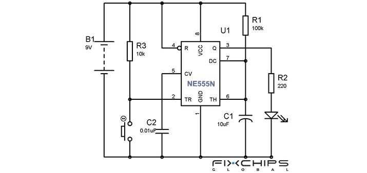
The NE555N is used in many practical electronic circuits. Its timing and switching functions allow it to control other components, such as LEDs, buzzers, transistors, and switching circuits.
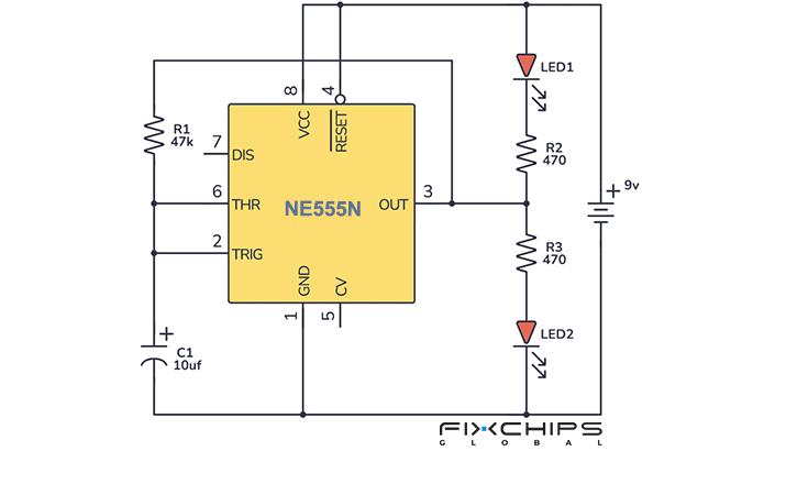
LED Flasher Circuits
The NE555N works in astable mode to generate a continuous pulse signal. The Output pin switches between high and low states, turning the LED on and off through a suitable current-limiting circuit. The timing resistor and capacitor determine the flashing rate.
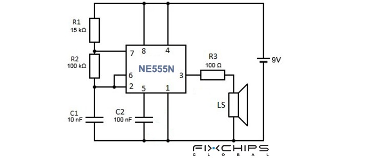
Tone Generation Circuits
In astable mode, the NE555N generates a repeating electrical signal at a selected frequency. This signal can drive a suitable buzzer or another sound-producing circuit. The timing resistor and capacitor determine the oscillation frequency and therefore affect the resulting tone.
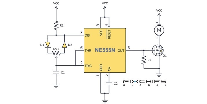
Motor Speed Control Circuits
The NE555N can be configured to generate a pulse-width-modulated signal for suitable motor-control circuits. The output signal controls a switching transistor or MOSFET, which regulates the power delivered to the motor. Changes in the pulse width affect the average voltage or power supplied to the motor, while the switching device handles the motor current.
Time-Delay Circuits
In monostable mode, the NE555N produces an output signal that stays high for a set period after receiving a trigger pulse. This output can control a transistor, relay driver, or other switching circuit. The external resistor and capacitor determine how long the controlled component remains active.
Frequently Asked Questions
Can the NE555N run from a 3V battery?
A standard bipolar NE555N is generally not designed to operate from a 3V supply. Its minimum supply voltage is commonly around 4.5V, so a 3V battery is usually below its specified operating range.
How does an NE555 Timer operate?
An NE555 Timer uses a voltage divider, two comparators, an SR flip-flop, a discharge transistor, and an output stage to control the output signal. The comparators monitor the input and timing voltages, while the flip-flop and output stage change the output state according to these voltage levels.
What is the difference between NE555 and NE555N?
NE555 and NE555N generally refer to the same basic bipolar 555 timer family, while the additional letter or suffix can identify a specific package or ordering version. The exact difference depends on the manufacturer and part-number system, so the corresponding datasheets should be checked before making a direct replacement.
Why does an NE555N stop working at low voltage?
A standard bipolar NE555N may stop working properly when its supply voltage falls below its specified minimum operating voltage. At a low supply voltage, the internal comparators and other circuit blocks may no longer operate within their specified conditions, which can cause unstable or incorrect output behavior.
Is the NE555 the same as the LM555?
The NE555 and LM555 are both members of the bipolar 555 timer family and have very similar basic functions and pin configurations. However, they can have differences in electrical specifications, operating conditions, or package options, so the datasheets should be compared before treating them as direct substitutes.


