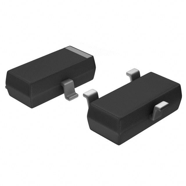
Vishay SI2309CDS-T1-GE3
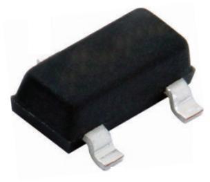
Image is only for reference















| Attribute | Value |
|---|---|
| HTS | COMPONENTS |
| PPAP | No |
| EU RoHS | Compliant |
| Category | Power MOSFET |
| Mounting | Surface Mount |
| ECCN (US) | EAR99 |
| Packaging | Tape and Reel |
| Pin Count | 3 |
| Automotive | No |
| Lead Shape | Gull-wing |
| PCB changed | 3 |
| Availability | No Stock Available |
| Channel Mode | Enhancement |
| Channel Type | P |
| Configuration | Single |
| Package Width | 1.3 |
| Package Height | 0.95 |
| Package Length | 2.92 |
| Supplier Package | SOT-23 |
| Maximum IDSS (uA) | 1 |
| Process Technology | TrenchFET |
| Standard Package Name | SOT |
| Manufacturer Lead Time | 42 weeks |
| Typical Fall Time (ns) | 10 |
| Typical Rise Time (ns) | 35 |
| Number of Elements per Chip | 1 |
| Maximum Power Dissipation (mW) | 1000 |
| Typical Gate Charge @ Vgs (nC) | [email protected] |
| Maximum Gate-Source Voltage (V) | ±20 |
| Typical Output Capacitance (pF) | 28 |
| Typical Turn-On Delay Time (ns) | 40 |
| Maximum Drain-Source Voltage (V) | 60 |
| Typical Gate Plateau Voltage (V) | 3 |
| Typical Turn-Off Delay Time (ns) | 15 |
| Maximum Diode Forward Voltage (V) | 1.2 |
| Typical Diode Forward Voltage (V) | 0.8 |
| Typical Gate to Drain Charge (nC) | 1.2 |
| Maximum Gate Threshold Voltage (V) | 3 |
| Minimum Gate Threshold Voltage (V) | 1 |
| Typical Gate to Source Charge (nC) | 0.8 |
| Typical Reverse Recovery Time (ns) | 30 |
| Maximum Operating Temperature (°C) | 150 |
| Minimum Operating Temperature (°C) | -55 |
| Maximum Continuous Drain Current (A) | 1.6 |
| Operating Junction Temperature (°C) | -55 to 150 |
| Typical Input Capacitance @ Vds (pF) | 210@30V |
| Typical Reverse Recovery Charge (nC) | 33 |
| Maximum Drain-Source Resistance (mOhm) | 345@10V |
| Maximum Gate-Source Leakage Current (nA) | 100 |
| Maximum Positive Gate-Source Voltage (V) | 20 |
| Maximum Pulsed Drain Current @ TC=25°C (A) | 8 |
| Typical Drain-Source Resistance @ 25°C (mOhm) | [email protected]|285@10V |
| Maximum Power Dissipation on PCB @ TC=25°C (W) | 1 |
| Typical Reverse Transfer Capacitance @ Vds (pF) | 20@30V |
| Maximum Continuous Drain Current on PCB @ TC=25°C (A) | 1.2 |
| Maximum Junction Ambient Thermal Resistance on PCB (°C/W) | 166 |
Purchase & Inquiry
You can place an order with FIXCHIPS without having to register or create an account.
To make payment more convenient, we support multiple payment methods in USD, including PayPal, credit cards, and wire transfer.
We suggest submitting an RFQ to get the most up-to-date pricing and availability for the components you are looking for. Our sales team will reply by email within 24 hours.
1. An email containing your order details will be sent to your inbox. If you cannot find it, please check your spam or junk mail folder.
2. Product availability and pricing may change over time. Our sales manager will verify the details of your order and contact you if any changes or confirmation are required.
Packaging Process